Estimating Flash Media Performance For Embedded Systems
by Yingbo Hu, R&D Embedded Software Engineer
Flash media are used by embedded systems to store program code, configuration information, tables, and various data. There are different kinds of flash media that can be used for this purpose. Besides cost and capacity of the flash media, performance is also an important factor especially for applications, which require recording streaming audio or video or real time logging of high-speed data. This article provides ideas and examples of how to estimate read and write performance; it should be helpful for selecting hardware and software.
There are two types of flash media for embedded systems. One type is raw flash memory, which directly connects to a microprocessor via a processor bus. NOR and NAND flash chips belong to this category. To support raw flash memory, you need a flash driver, which will handle the details of the flash media such as read/write, logical to physical address translation, bad block handling, wear leveling, and garbage collection (recycling of used blocks). The other type of flash media is called managed flash media. It connects to a microprocessor through a peripheral bus such as USB, MMC/SD, or CompactFlash. On the processor side, you need software such as a USB host stack or a MMC/SD driver to interface to the flash media. Normally you dont need to know the details of flash memory.
To estimate the performance of a flash media, it is first necessary to determine the physical limitations of the chip and then estimate the overhead introduced by the hardware and software. Physical limitations vary from vendor to vendor and between parts from the same vendor. Hardware overhead normally is related to processor bus speed and external RAM speed. (Data is normally transferred from the flash media to or from external RAM via the processor bus.) Software overhead is related to the software design and instruction execution times. Two example calculations are provided below: one for NAND flash and one for an SD card.
1. NAND Flash Memory Chip
A NAND flash memory chip can be connected directly to the main processor bus. Most NAND flash are either 8 bit or 16 bit devices so each read/write cycle can only read or write 8 or 16 bits from or to flash memory. NAND flash memory has no address input like RAM; it requires a special address/command cycle to start a data transfer. Then a page of data is transferred. Page size varies with the size of the NAND chip. It can be 512, 2048, or 4096 data bytes for current chips. Additional control bytes are added to these, so the full page size is a number such as 2112 bytes.
1.1 Physical Limitation.
The following is an example of a detailed analysis, based upon vendor documentation, to determine the maximum data transfer rates for an 8 Gbit, 8 bit SLC NAND flash chip. First we will list the AC characteristics and then we will calculate the read and write limitations imposed by the timing data.
AC Characteristics: Command, Data, and Address Input
| Parameter |
Symbol |
Min |
Max |
Unit |
| ALE to data start |
tADL |
70 |
- |
ns |
| ALE hold time |
tALH |
5 |
- |
ns |
| ALE setup time |
tALS |
10 |
- |
ns |
| CE# hold time |
tCH |
5 |
- |
ns |
| CLE hold time |
tCLH |
5 |
- |
ns |
| CLE setup time |
tCLS |
10 |
- |
ns |
| CE# setup time |
tCS |
15 |
- |
ns |
| Data hold time |
tDH |
5 |
- |
ns |
| Data setup timet |
tDS |
10 |
- |
ns |
| Write cycle time |
tWC |
25 |
- |
ns |
| WE# pulse width HIGH |
tWH |
10 |
- |
ns |
| WE# pulse width |
tWP |
70 |
- |
ns |
AC Characteristics: Normal Operation
| Parameter |
Symbol |
Min |
Max |
Unit |
| ALE to RE# delay |
tAR |
10 |
- |
ns |
| CE# access time |
tCEA |
- |
25 |
ns |
| CE# HIGH to output High-Z |
tCHZ |
- |
30 |
ns |
| CLE to RE# delay |
tCLR |
10 |
- |
ns |
| CE# HIGH to ouput hold |
tCOH |
15 |
- |
ns |
| Cache busy in page read chace mode (first 31h) |
tDCBSYR1 |
- |
3 |
μs |
| Cache busy in page read chace mode (next 31h and 3Fh) |
tDCBSYR2 |
DCBSYR1 |
25 |
μs |
| Output High-Z to RE# LOW |
tIR |
0 |
- |
ns |
| Data transfer from Flash array to data register |
tR |
- |
25 |
μs |
| READ cycle time |
tRC |
25 |
- |
ns |
| RE# access time |
tREA |
- |
20 |
ns |
| RE# HIGH hold time |
tREH |
10 |
- |
ns |
| RE# HIGH to ouput hold |
tRHOH |
15 |
- |
ns |
| RE# HIGH to WE# LOW |
tRHW |
100 |
- |
ns |
| RE# HIGH to output High-Z |
tRHZ |
- |
100 |
ns |
| RE# LOW to ouput hold |
tRLOH |
5 |
- |
ns |
| RE# pulse width |
tRP |
12 |
- |
ns |
| Ready to RE# LOW |
tRR |
20 |
- |
ns |
| Reset time (READ/PROGRAM/ERASE) |
tRST |
- |
5/10/500 |
μs |
| WE# HIGH to gusy |
tWB |
- |
100 |
ns |
| WE# HIGH to RE# LOW |
tWHR |
60 |
- |
ns |
PROGRAM/ERASE Characteristics
Symbol |
Parameter |
Typ |
Max |
Unit |
NOP |
Number of partial-page programs |
- |
4 |
cycles |
tBERS |
BLOCK ERASE operation time |
0.5 |
3 |
ms |
tPROG |
PROGRAM PAGE operation time (1.8V) |
300 |
600 |
μs |
tPROG |
PROGRAM PAGE operation time (3.3V) |
220 |
500 |
μs |
Each NAND flash page read/program operation may be split into operation cycles and busy time. They are Command Latch Cycle, Address Latch Cycle, Input Data Latch Cycle, Data Transfer from Flash Array to Register Busy Time, Serial Access Cycle, Program Busy Time. The following are the waveforms of those cycles.
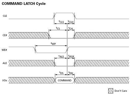
The time duration to complete one command cycle is tWP + max(tCLH, tCH, tALH, tDH) = 12 + max(5, 5, 5, 5, 5) = 17 ns.
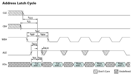
The time duration to complete 5 address cycles is 5*tWC + (tCS-tWP ) = 5*25 + (15-12) = 128 ns.
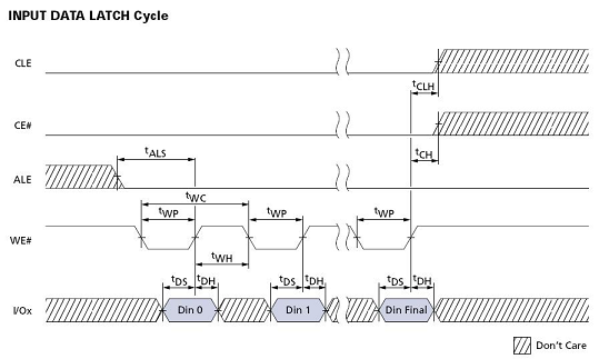
The time duration to complete one page (2112 bytes) of write data cycles is 2112*tWC + max(tCLH, tCH, tDH) = 2112*25 + max(5, 5, 5) = 52805 ns = 52.805 µs.
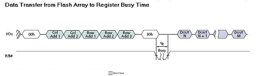
The time for the Data Transfer from Flash Array to Register is tR= 25 µs.
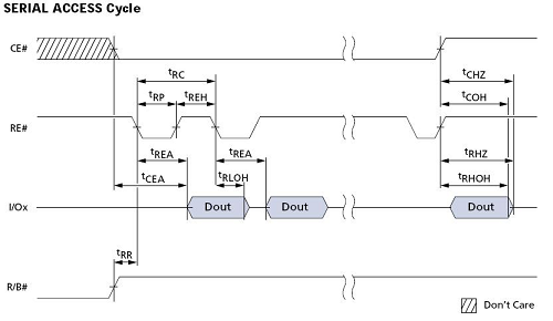
The time duration to complete one page (2112 bytes) of read data cycles is 2112*tRC + tRR = 2112*25 + 20 = 52820ns = 52.82 µs.
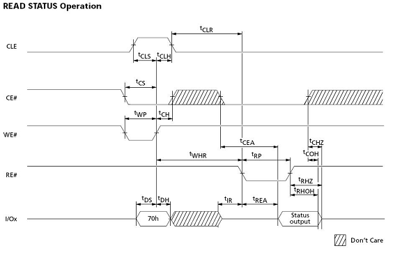
The time duration to check program/erase status is tCS + tCLH + tCLR + tRP + tRHZ =15 + 5 +10 + 12 + 100 = 142 ns.

The Program Busy time is tPROG = 220 µs.
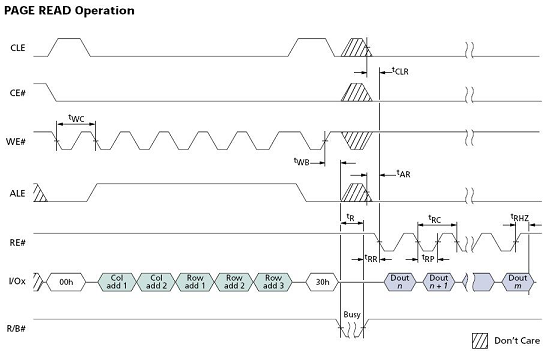
The following timing diagram shows what is necessary to read one page of data.
All though the actual data area is 2048 byte, normally driver software will store meta data in the spare area of each page such as the logical page address and ECC data. Hence, we will use the full page data size of 2112 bytes instead of the data area size of 2048 bytes to calculate the time for a read operation. (Note: reading the spare area with a separate operation would introduce extra overhead.)
Reading one page requires: one COMMAND LATCH Cycle (Read command 00), 5 Address Latch cycles, another COMMAND LATCH Cycle (Read command 30h), data transfer from the flash array to register tR, and 2112 SERIAL ACCESS cycles. The total time duration is: 17 + 128 + 17 + 25,000 + 52,820 = 77,982ns. The total physical read performance limitation is therefore: 2112/77,982ns = 27,083,173 bytes/second = 27.08 MB/sec. As can be seen, the main factors determining read performance are data transfer time from the flash array to register and data access time.
The following timing diagram shows what is necessary to program (write) one page of data
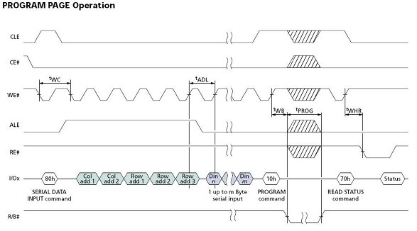
Writing one page requires: one COMMAND LATCH cycle (Program Page command 80h), 5 Address Latch cycles, ALE to data start time tADL, 2112 INPUT DATA LATCH cycles, another COMMAND LATCH cycle (Program command 10h), Program Time tPROG and Read Status Operation. The total time duration is 17 + 128 + 52,805 + 17 + 220,000 + 17 + 142 = 27,3126ns. The total physical write performance limitation is 2112/27,3126ns = 7,732,695byte/second = 7.73 MB/s. As can be seen, the main factors determining write performance are Program time and Data Input time.
1.2 Hardware overhead
The above calculations provide theoretical upper limits for read and write operations. The microprocessor usually adds additional hardware overhead. For example, if the external bus speed is less than 40MHz (25ns read/write cycle) assumed above. This is common for low-end microprocessors, such as most ARM7 processors, for which the CPU clock rate is only 72 MHz and internal bus clock is only 36 MHz. The external bus clock is even slower. When calculating this kind of overhead, we mustadjust the tWC and tRC values in the above formulations to be the actual bus speed of the processor.
The following is an example of how to calculate the NAND flash bus speed. This is using an ATMEL SAM9263, which is actually an ARM9 processor. The NAND flash chip is connected to the EBI (External Bus Interface).

MCK is set to 120MHz. The minimum working NRD_CYCLE is 8 so each NAND flash read operation requires 8 MCK cycles, which total 67ns. This is far longer than the minimum 25 ns cycle time of the flash memory chip. Hence, performance is reduced by a factor of 67/25 = 2.68! The theoretical maximum performance for the above NAND chip, when used with this processor, is 25.8/2.68 = 9.6 MB/sec. Using DMA will not improve this, since it is a fundamental bus bandwidth limitation.
In addition, if you store your data in an SDRAM, the SDRAM bus will cause extra hardware overhead. The following is an SDRAM read bus timing for ATMEL SAM9263.
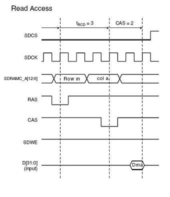
SDCK is 100MHz and each read operation needs 5 SDCK cycles. Hence, to read one byte of data from the SDRAM (NAND flash bus width is 8 bits) requires 50 ns, so the theoretical maximum performance for the SDRAM to store the NAND flash data is 20MB/sec.
The above NAND flash bus overhead and SDRAM bus overhead add to software overhead as shown below.
1.3 Software overhead
Software also adds overhead for flash reads and writes. The software structure for a flash file system is as shown below.
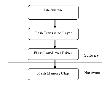
The file system calls the Flash Translation Layer (FTL) to map the logical sector address, which it provides, to the flash memorys physical sector address. Then, the Flash Low-Level Driver tranfers data to and from the flash memory chip. This layer is also known as the Hardware Adaptation Layer (HAL).
The flash low level driver is pretty simple so it is possible to calculate its overhead based upon the generated assembly code. For example, we are using the following C language code to read one page of data:
unsigned char *p = read_data, *p0 = read_data + page_size;
    for(; p < p0; p++)
    {
        *p = *(volatile unsigned char*)(DATA_PORT);
    }
The IAR compiler generates the following assembly code:
//     unsigned char *p = read_data, *p0 = read_data + page_size;
        MOVS     R4,R1
        ADDS     R0,LR,R1
        MOVS     R5,R0
//     for(; p < p0; p++)
       ?? Read_Page_5:
        CMP      R4,R5
        BCS      ?? Read_Page_6
//         {
//           	*p = *(volatile unsigned char*)(DATA_PORT);
    			MOV      R0,#+1073741824
    			LDRB     R0,[R0, #+0]
    			STRB     R0,[R4, #+0]
//         }
        ADDS     R4,R4,#+1
        B        ?? Read_Page_5
So the loop to read one byte requires 7 instructions. If the processor is running at 200MHz, then the processor needs 7*5 ns = 35 ns to read one byte of data. This is longer than the minimum 25 ns cycle time of the flash memory chip. Software overhead, in this case, is 40%.
Hardware overhead must be added to the software overhead. For example,
LDRB R0,[R0, #+0]
reads one byte of data from the NAND flash bus, so an additional 67 ns NAND flash bus hardware overhead must be added. Then,
STRB R0,[R4, #+0]
saves the data byte to SDRAM, so additional an additional 50 ns SDRAM bus hardware overhead must be added. Therefore, the total time to read one byte from the NAND flash is 35ns + 67ns + 50ns = 152ns. This gives a performance limit of 6.5 MB/sec. This compares to the theoretical NAND flash limit of 27.08 MB/sec, which was calculated above. Hence, actual performance has been reduced by 76% due to hardware and software overhead! SDRAM needs to be refreshed periodically, so long-term performance is even less.
Using DMA to transfer data will reduce the software overhead. Test results show DMA can reduce software overhead by 50% or more, but hardware overhead due to bus speed limitations cannot be reduced by DMA.
The file system and FTL are too complex to calculate their overheads. The best way to proceed is to measure flash driver performance alone, then measure it with FTL, and then measure it with both FTL and the file system. The following table is an example of this for an ATMEL SAM9263EVB board with 256 MB NAND flash.
K9F2G08U on SAM9263 |
Reading (KB/s) |
Read Percentage |
Writing (KB/s) |
Writing Percentage |
Flash Low Level Driver |
5041 |
100% |
4161 |
100% |
smxNAND Flash Driver |
4266 |
85% |
1969 |
47% |
smxFS with Flash Driver |
3373 |
67% |
1689 |
41% |
We can see from the above table that performance reduction is very significant for software. Comparing to the previous 27.08 MB/sec theoretical limit, final file system performance is only 12.4% an 8:1 reduction!
2. SD Card
An SD card is an example of a managed flash media. It transfers data through an MMC/SD card bus, which is controlled by an MMC/SD card controller. (Another conncection method is an SPI bus controlled by an SPI bus controller.) The SD specification defines two card bus modes: 1 bit or 4 bit. The SD specification also defines the SD bus speed limitation. For an SD v1.0 or v2.0 normal speed card, the maximum BUS clock is 24MHz; an SD v2.0 high speed card supports up to 50 MHz bus speed.
2.1 Physical Limitation
The following is a timing diagram for an SD Block Read command.

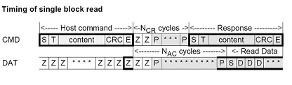
The time duration for reading one block of data includes the time for sending the block read command, receiving the response, and reading the data block with CRC. Because the command and response are short compared with the transfer of a data block, we can ignore them when we calculate the physical limitation. For 1-bit mode (also true for SPI mode), SD normal speed card reading speed is 24 MB/8 = 3 MB/sec. For 4-bit mode, SD normal speed card reading speed is 24 MB/2 = 12 MB/sec. High speed card reading speed is 50 MB/2 = 25 MB/sec.
The following is a timing diagram for an SD Block Write command:
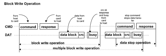
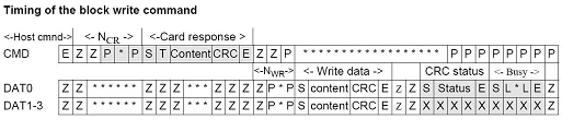
The time duration for writing one block of data includes the time for sending the block write command, receiving the response, sending the data block with CRC, and waiting for card busy. Because the command and response are short compared with the transfer of a data block, we can ignore them when we calculate the physical limitation.
Unlike block read, block write needs additional time to complete because the card needs to program the data into the flash memory. That is the busy time shown in the diagram. Busy time varies from card to card from different vendors. There is no specification for this value so it is necessary to measure it. Block write speed should definitely slower than the read speed so for 1-bit mode, SD normal speed card writing speed is far less than 3 MB/sec; 4-bit mode is less than 12 MB/sec; and high speed card writing speed is less than 25 MB/sec.
2.2 Hardware overhead
As with a NAND flash memory chips, the microprocessor may generate additional hardware overhead. For example, the MMC/SD card controller may not set the clock to the maximum speed defined by the SD specification. If the processors peripheral block clock is 40MHz and the divider can only be an integer, then it is not possible to get a 24MHz SD bus clock; 20MHz is the closest possible a 17% reduction in performance. The MMC/SD controller will also introduce some overhead. For example, generating and checking CRC fields of data and command packets reduces performance.
2.3 Software overhead
Software also introduces overhead. As in the NAND case, for a write operation, code is needed to transfer data to the MMC/SD controllers FIFO. Using DMA can reduce this overhead, but not eliminate it entirely. An MMC/SD card does not require a flash translation layer and an MMC/SD memory card driver is fairly simple so the software overhead is a little smaller than for a NAND chip.
The following is an example for an ATMEL SAM9RL64EVB board with a 512 MB and a 2GB SD card. Both cards are working for 4-bit bus mode. The highest possible SD clock bus clock rate is 20 MHz. The driver is using DMA to transfer data between the processors RAM and the SD controller in order to reduce software overhead. Even so, for read, the raw data rate for the SD card is over 10 MB/s but at the file system level, maximum performance is about 5 MB/s only 50% of raw data performance. Software overhead is the main factor for this performance degradation.
For write, the file system achieves 64% of the raw data performance. In this case, the hardware overhead is more important. Note, however, that write performance is much less than read performance due to SD card busy time mentioned above. A word of caution concerning managed flash media is that they require garbage collection just like raw NAND. (Garbage collection is the process of erasing used blocks that are no longer needed in order to reuse them.) Erase times are typically long and can occur during write operations, potentially causing data overflows (if there is not enough RAM buffering.) The following are some sample measured times.
SanDisk UltraII 512M |
Reading |
Writing |
MMC/SD/SDHC driver raw data |
6554 KB/s |
5650 KB/s |
MMC/SD/SDHC driver and smxFS |
5094 KB/s |
3696 KB/s |
SanDisk 2GB |
Reading |
Writing |
MMC/SD/SDHC driver raw data |
10240 KB/s |
3724 KB/s |
MMC/SD/SDHC driver and smxFS |
5132 KB/s |
2348 KB/s |
back to White Papers page
|